


onsemi NCP4306 Synchronous Rectification Drivers

onsemi NCP4306 Synchronous Rectification Drivers are high‑performance secondary‑side devices designed to optimize efficiency in switch‑mode power supplies (SMPS). The onsemi NCP4306 supports a wide range of power‑conversion topologies (including DCM/CCM flyback, quasi‑resonant flyback, forward, and resonant LLC) thanks to the versatile control architecture and robust drive capability. These devices provide precise true secondary‑side zero‑current detection and offer extremely low turn‑off delay (typically 15ns), enabling maximum MOSFET conduction time and improved overall system efficiency. The combination of adjustable or fixed minimum on‑time and off‑time blanking allows designers to mitigate PCB‑induced ringing and parasitic effects for stable, noise‑free SR operation.
Additional features such as self‑synchronization, a rugged current‑sense pin rated up to 200V, high peak sink/source drive capability (7A/2A), automatic light‑load disable mode, and a 5V gate clamp for GaN transistor compatibility make the NCP4306 suitable for demanding high‑efficiency applications. Typical uses include notebook adapters, high‑power‑density AC/DC chargers, LCD televisions, and other SMPS designs requiring top‑tier efficiency performance.
Features
- Self-contained control of synchronous rectifier in CCM, DCM, and QR for flyback or LLC applications
- Precise true secondary zero current detection
- 15ns typical turn-off delay from the current sense input to the driver
- Rugged current sense pin (up to 200V)
- Ultrafast (10.5ns) turn-off trigger interface/disable input
- Adjustable or fixed minimum ON-time
- Adjustable or fixed minimum OFF-time with ringing detection
- Improved robust self-synchronization capability
- 7A/2A peak current sink/source drive capability
- Operating voltage range up to VCC = 35V
- Automatic light-load disable mode
- GaN transistor driving capability
- Low startup and disable current consumption
- Up to 1MHz maximum operation frequency
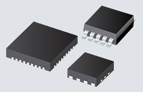
- Package options
- 4mm x 4mm DFN8
- 2.0mm x 2.2mm DFN8
- SOIC-8
- TSOP-6
- Lead-free
Applications
- Notebook adapters
- High power density AC/DC power supplies (cell phone chargers)
- LCD TVs
- All SMPS with high efficiency requirements
Specifications
- 35V maximum operating voltage
- Supply section
- 3.7V to 4.2V VCC UVLO rising range
- 3.2V to 3.7V VCC UVLO falling range
- 0.5V typical VCC UVLO hysteresis
- 80μs maximum start-up delay
- 2.2mA to 15mA current consumption range
- 60μA maximum current consumption below UVLO
- 80μA or 100μA maximum current consumption in disable mode
- Driver output
- 100ns maximum output voltage rise time
- 45ns maximum output voltage fall time
- 2Ω typical driver source resistance
- 0.5Ω typical driver sink resistance
- 2A typical output peak source current
- 7A typical output peak sink current
- 4ms (typical) maximum driver pulse length
- CS input
- 500nA maximum CS leakage current
- 0.5V to 3.0V typical dV/dt detector threshold voltage range
- 13ns to 37ns dV/dt detector threshold range
- ±15% exception timer ratio accuracy
- Trigger disable input
- 10ns (maximum) minimum trigger pulse duration
- 1.6V to 2.2V trigger threshold voltage range
- 16.5ns maximum trigger to DRV propagation delay
- 30ns to 80ns trigger blank time range after a DRV turn-on event
- 75µs to 125µs delay to disable mode range
- 3.0µs maximum disable recovery timer
- 200ns (maximum) minimum pulse duration to disable mode end
- 7µA to 15µA pull-down current range
- 10µs maximum transition time
- -40°C to +125°C operating junuction temperature range
- +150°C maximum junction temperature
- Junction-to-air thermal resistance
- 200°C/W for SOIC-8
- 250°C/W for TSOP-6
- 80°C/W for 4mm x 4mm DFN8
- 85°C/W for 2mm x 2.2mm DFN8
- ESD protection
- 2000V Human Body Model (except pin CS)
- 600V Human Body Model pin CS
- 200V Machine Model
- Class C3 Charged Device Model
Internal Circuit Architecture

Related Solutions

onsemi USB Type-C™ Solutions
Not only replacing older USB standards, but also other standards like Thunderbolt and DisplayPort.