


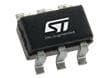
STMicroelectronics TSC240 Zero-Drift Current Sense Amplifiers

STMicroelectronics TSC240 Zero-Drift Current Sense Amplifiers are precision, bidirectional amplifiers designed for high-accuracy current measurement in industrial and consumer applications. Operating over a 2.7V to 5.5V supply voltage range, the STMicroelectronics TSC240 amplifiers support both high-side and low-side current sensing with excellent common-mode rejection. These devices feature a low input offset voltage and minimal drift over temperature, thanks to zero-drift architecture, ensuring stable and reliable performance across varying conditions. With a preset gain of 20V/V, the TSC240 offers flexibility for different sensing requirements. Housed in compact SO8 or TSSOP8 packages, the TSC240 amplifiers are ideal for use in power management systems, motor control, and battery-operated devices where precision and efficiency are critical.
Features
- Enhanced PWM rejection
- Excellent 132dB DC CMRR
- Wide -4V to 100V common-mode range
- 20V/V available gain
- Gain accuracy
- 0.20% maximum error
- 2.5ppm/°C maximum drift
- Offset accuracy
- ±20μV maximum voltage
- 150nV/°C maximum drift
- 2.4mA maximum quiescent current
- SO8 and TSSOP8 package options
- RoHS compliant
Applications
- Motor controls
- Solenoid and valve controls
- Power management
- Industrial process control
- Telecom equipment
Specifications
- 2.7V to 5.5V operating supply voltage range
- -4V to +100V operating common-mode voltage range on the input pins
- 2.4mA to 2.6mA maximum power supply current consumption range
- Input
- 20µV to 56µV maximum offset voltage range
- 150nV/°C maximum offset drift vs. temperature
- 75dB to 132dB typical common-mode rejection range
- 150µA to 250µA maximum input bias current range
- 120dB typical supply voltage rejection
- Output
- 20V/V typical gain
- ±0.20% maximum gain error
- ±2.5ppm/°C maximum gain error vs. temperature
- ±0.001% typical non-linearity error
- 30mV typical output swing to the positive rail
- 4mV typical output swing to GND
- 30mA to 50mA maximum output current range
- 1.5VmV/mA maximum load regulation
- 2.2nF maximum capacitive load
- Offset adjustment
- 20µV/V typical reference voltage rejection ratio
- 0.1% typical reference divider accuracy
- Dynamic performance
- 100kHz to 560kHz typical bandwidth range
- 2V/µs typical slew rate
- 5µs typical settling time
- 2.5µs typical PWM rejection settling time
- 50nV/√Hz typical voltage noise density
- ESD ratings
- 2000V Human Body Model (HBM)
- Charged Device Model (CDM)
- 1000V for the SO8
- 750V for the TSSOP8
- Maximum junction-to-ambient thermal resistance
- 125°C/W for the SO8
- 120°C/W for the TSSOP8
- -40°C to +125°C operating free-air temperature range
- +150°C maximum junctin temperature
Block Diagram

Videos
Related Amplifiers

STMicroelectronics TSC202x Bidirectional Current Sense Amplifiers
Senses current via a shunt resistor over a wide range of common-mode voltages, from -4V to +100V.

STMicroelectronics TSC200, TSC201, & TSC202 Amplifiers
A high-side current sense amplifier that delivers an analog voltage output.

STMicroelectronics TSC201x Bidirectional Current Sense Amplifiers
Bidirectional current sense amplifier with a -20V to +70V common-mode voltage range.
STMicroelectronics TSC210 Current Sense Amplifiers
Zero-drift current sense amplifiers that can sense current via a shunt resistor.

STMicroelectronics TSC21x Current Sense Amplifiers
Low-/high-side, bidirectional current sense amplifier featuring zero-drift architecture.
Complete Your Design

STMicroelectronics Standard Products
A broad range of drop-in replacements for general-purpose analog ICs, discretes, and serial EEPROMs.